Semiconductor
Semiconductor Industry
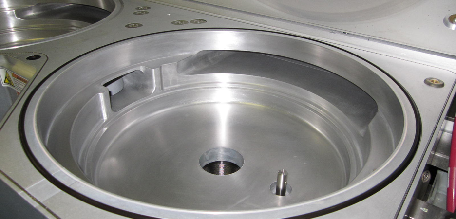
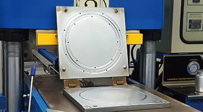
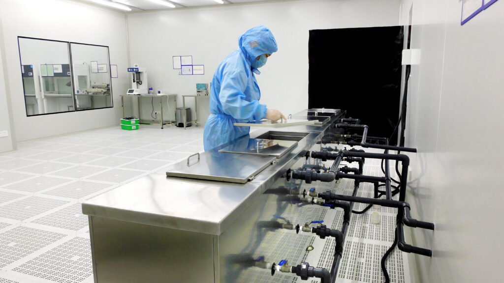
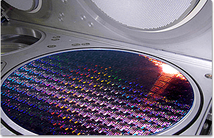
With years of industry experience, Boilpeak has earned the trust of leading semiconductor wafer fabs and equipment manufacturers by providing reliable, efficient, and cost-saving solutions for their critical applications. Boilpeak’s fluorinated elastomer seals are manufactured in a high-specification environment that exceeds cleanroom standards, with R&D efforts continually evolving to meet the cutting-edge technologies.
We have introduced a series of dedicated applications to satisfy the rapidly changing demands of the semiconductor industry. Boilpeak’s related fluorinated sealing products utilize special fluorinated polymerization technology, making them effectively applicable in the latest advanced processes such as reactive ion etching and chemical deposition. As these industries continue to evolve, we remain committed to advancing alongside them in these technological sectors.

O-rings maximize equipment performance.

Meeting the Challenges of Semiconductor Sealing
Provides the most comprehensive sealing combination
We offer the most comprehensive seal portfolio using proprietary polymer and process technologies, as well as a wide range of compression molding capabilities, and we offer customized solutions for the most critical applications in advanced processes.

High-Standard Quality Inspection and Control
- Continuous innovation
- Continuous supply of supplies
Boilpeak is dedicated to developing an extensive range of innovative sealing materials and products, providing exceptional sealing integrity in the most demanding semiconductor manufacturing environments. The semiconductor industry has specific requirements for O-rings that can resist high temperatures and chemicals.
Process Application
Boilpeak boasts over 10 years of exceptional manufacturing experience. With the continuous development and innovation of the industry, and in the face of rigorous manufacturing conditions, we are committed to providing various solutions. We continually develop new special elastomer materials while simultaneously offering optimal sealing solutions.

Thin Film Process
The thin film process can be divided into two deposition methods: CVD (Chemical Vapor Deposition) and PVD (Physical Vapor Deposition). Both deposition methods pose different challenges for sealing applications in the process.

Etching Process
The etching process environment is categorized into Dry Etching and Wet Etching. The primary use of high-intensity plasma and various chemicals in the etching process poses different challenges for sealing applications.

Diffusion Process
The diffusion process can be divided into Ion Implantation and Diffusion. The primary use of extremely high temperatures and various chemicals in the diffusion process poses different challenges for sealing applications.